
Introduction
Semiconductor Yield Management Software plays a critical role in modern chip manufacturing. As process nodes shrink and designs become more complex, even small variations in fabrication can lead to significant yield loss. Yield management software helps semiconductor companies monitor, analyze, and improve manufacturing yield by turning massive volumes of fab data into actionable insights.
These platforms sit at the intersection of manufacturing execution systems (MES), process control, test data, and advanced analytics. They enable engineers and managers to quickly identify defect patterns, root causes, and process drifts that would otherwise remain hidden across thousands of wafers and billions of data points.
Why it matters:
Yield directly impacts profitability, time-to-market, and product quality. Improving yield by even a small percentage can save millions of dollars per production line while improving customer satisfaction and supply stability.
Common real-world use cases include:
- Early detection of yield excursions
- Root cause analysis of defects and failures
- Process optimization across fabs and nodes
- Test data correlation and binning analysis
- Continuous yield monitoring and reporting
Key evaluation criteria when choosing yield management software:
- Depth of yield analytics and root cause capabilities
- Scalability for high-volume fab data
- Integration with MES, test, and inspection tools
- Ease of use for engineers and analysts
- Security, compliance, and enterprise readiness
Best for:
Process engineers, yield engineers, data scientists, fab managers, and semiconductor manufacturers ranging from advanced logic fabs to memory, analog, and specialty device producers.
Not ideal for:
Small electronics companies without in-house manufacturing, early-stage startups that outsource all fabrication, or teams that only require basic statistical process control rather than full yield analytics.
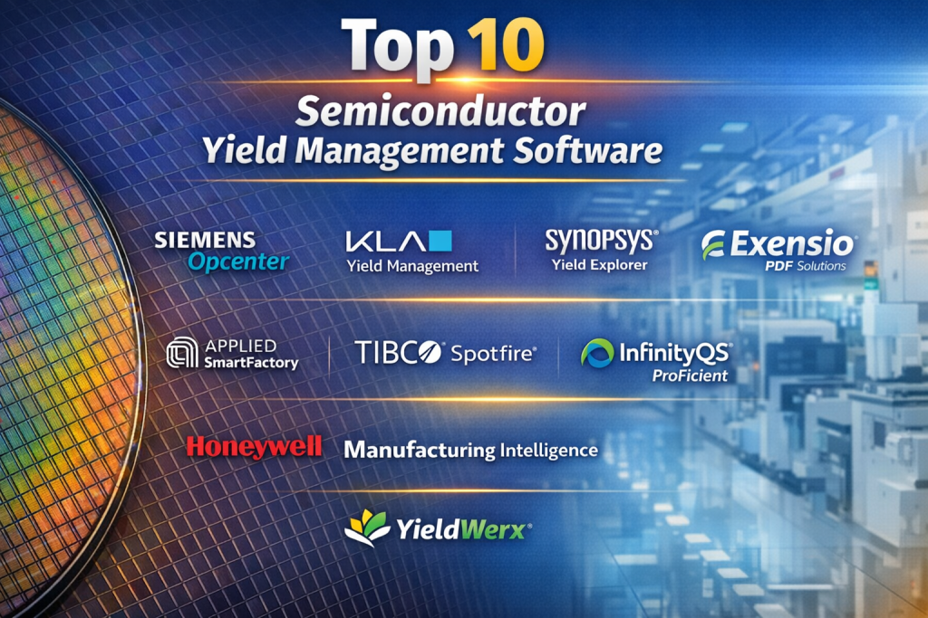
Top 10 Semiconductor Yield Management Software Tools
1 — Siemens Opcenter
Short description:
Siemens Opcenter provides enterprise-grade manufacturing analytics with strong yield management and process intelligence capabilities, designed for large semiconductor fabs and global manufacturers.
Key features:
- Advanced yield analytics and dashboards
- Integration with MES and shop-floor systems
- Statistical process control (SPC)
- Root cause analysis and defect tracking
- Cross-fab data harmonization
- Scalable big data architecture
Pros:
- Very strong enterprise integration
- Proven reliability in high-volume fabs
Cons:
- Complex implementation
- High cost for smaller organizations
Security & compliance:
Enterprise-grade security, role-based access, audit trails, ISO-aligned practices.
Support & community:
Extensive documentation, global enterprise support, professional services-led onboarding.
2 — KLA Yield Management
Short description:
KLA Yield Management solutions are deeply embedded in semiconductor inspection and metrology ecosystems, offering best-in-class defect and yield analytics.
Key features:
- Defect density and pattern analysis
- Inline and offline inspection integration
- Wafer-level yield dashboards
- Advanced visualization tools
- AI-assisted root cause analysis
Pros:
- Industry-leading defect analytics
- Tight integration with inspection tools
Cons:
- Limited flexibility outside KLA ecosystem
- Premium pricing
Security & compliance:
Strong enterprise security, access controls, and audit logging.
Support & community:
High-touch enterprise support and domain-specific expertise.
3 — Synopsys Yield Explorer
Short description:
Synopsys Yield Explorer focuses on advanced yield learning by correlating test, design, and manufacturing data for faster ramp-up and optimization.
Key features:
- Test and yield data correlation
- Advanced analytics and modeling
- Design-for-manufacturability insights
- High-performance data processing
- Customizable reporting
Pros:
- Excellent for design-to-manufacturing feedback
- Strong analytics depth
Cons:
- Steeper learning curve
- Less intuitive UI for new users
Security & compliance:
Enterprise-grade security, encryption, and access management.
Support & community:
Strong technical documentation and enterprise customer support.
4 — PDF Solutions Exensio
Short description:
Exensio is a widely used yield management and analytics platform known for deep yield learning and cross-fab data visibility.
Key features:
- Yield learning and excursion detection
- Cross-fab and multi-node analytics
- Data normalization and harmonization
- Predictive yield modeling
- Collaboration tools for engineers
Pros:
- Proven yield improvement results
- Scales well across global fabs
Cons:
- Implementation can be lengthy
- Requires skilled users for advanced analytics
Security & compliance:
Enterprise security, audit logs, and access controls.
Support & community:
Strong professional services and domain-specific support.
5 — Applied Materials SmartFactory
Short description:
SmartFactory Yield solutions focus on intelligent manufacturing and yield optimization using AI-driven insights.
Key features:
- AI-based yield optimization
- Real-time manufacturing analytics
- Process drift detection
- Integrated fab intelligence
- Predictive analytics
Pros:
- Strong AI and automation capabilities
- Optimized for advanced fabs
Cons:
- Tied closely to Applied Materials ecosystem
- High cost
Security & compliance:
Enterprise security standards, encrypted data handling.
Support & community:
Enterprise-grade global support and consulting services.
6 — TIBCO Spotfire
Short description:
TIBCO Spotfire is a powerful analytics platform often customized for semiconductor yield analysis and visualization.
Key features:
- Advanced data visualization
- Real-time analytics dashboards
- Statistical analysis tools
- Integration with fab data sources
- Custom scripting and automation
Pros:
- Highly flexible analytics
- Strong visualization capabilities
Cons:
- Requires customization for yield workflows
- Not semiconductor-specific out of the box
Security & compliance:
SSO support, role-based access, enterprise security features.
Support & community:
Large user community, extensive documentation, enterprise support.
7 — InfinityQS ProFicient
Short description:
InfinityQS ProFicient emphasizes statistical process control and yield improvement for manufacturing environments.
Key features:
- Real-time SPC monitoring
- Yield and quality analytics
- Automated alerts and rules
- Integration with MES systems
- Compliance reporting
Pros:
- Strong SPC focus
- Easier adoption compared to heavy platforms
Cons:
- Limited advanced yield learning
- Less suitable for cutting-edge nodes
Security & compliance:
Audit trails, role-based access, compliance reporting.
Support & community:
Good documentation and responsive customer support.
8 — Camstar Analytics
Short description:
Camstar Analytics provides yield and process insights tightly coupled with MES workflows.
Key features:
- MES-integrated yield analysis
- Process performance dashboards
- Defect and scrap tracking
- Configurable reports
- Scalable architecture
Pros:
- Strong MES alignment
- Reliable enterprise performance
Cons:
- Less advanced AI analytics
- UI can feel dated
Security & compliance:
Enterprise security and compliance standards.
Support & community:
Strong enterprise support ecosystem.
9 — Honeywell Manufacturing Intelligence
Short description:
Honeywell Manufacturing Intelligence supports yield and quality analytics across complex manufacturing operations.
Key features:
- Yield and quality analytics
- Process optimization tools
- Data integration across plants
- Predictive analytics
- Reporting and dashboards
Pros:
- Strong industrial analytics foundation
- Scales well across sites
Cons:
- Semiconductor-specific features may require customization
- Longer deployment cycles
Security & compliance:
Enterprise-grade security and compliance frameworks.
Support & community:
Global enterprise support and training programs.
10 — YieldWerx
Short description:
YieldWerx is a focused yield analytics solution designed for semiconductor test and yield engineers.
Key features:
- Test data analysis
- Yield binning and correlation
- Custom dashboards
- Fast data ingestion
- Engineer-friendly workflows
Pros:
- Practical and engineer-centric
- Faster setup compared to enterprise suites
Cons:
- Limited enterprise-scale features
- Smaller ecosystem
Security & compliance:
Varies / N/A depending on deployment model.
Support & community:
Smaller but responsive support team and targeted documentation.
Comparison Table
| Tool Name | Best For | Platform(s) Supported | Standout Feature | Rating |
|---|---|---|---|---|
| Siemens Opcenter | Large enterprise fabs | On-prem / Hybrid | MES-integrated yield analytics | N/A |
| KLA Yield Management | Inspection-driven yield | On-prem | Defect pattern expertise | N/A |
| Synopsys Yield Explorer | Design-to-manufacturing | On-prem | Design-yield correlation | N/A |
| PDF Solutions Exensio | Yield learning at scale | On-prem / Hybrid | Cross-fab analytics | N/A |
| Applied Materials SmartFactory | AI-driven fabs | On-prem | Predictive yield AI | N/A |
| TIBCO Spotfire | Custom analytics teams | Cloud / On-prem | Advanced visualization | N/A |
| InfinityQS ProFicient | SPC-focused fabs | On-prem / Cloud | Real-time SPC | N/A |
| Camstar Analytics | MES-centric operations | On-prem | Process visibility | N/A |
| Honeywell Manufacturing Intelligence | Multi-site manufacturers | Hybrid | Industrial analytics | N/A |
| YieldWerx | Yield engineers | On-prem | Fast test data insights | N/A |
Evaluation & Scoring of Semiconductor Yield Management Software
| Criteria | Weight | Evaluation Notes |
|---|---|---|
| Core features | 25% | Depth of yield analytics, RCA, SPC |
| Ease of use | 15% | UI clarity, learning curve |
| Integrations & ecosystem | 15% | MES, test, inspection compatibility |
| Security & compliance | 10% | Access control, auditability |
| Performance & reliability | 10% | Handling high-volume fab data |
| Support & community | 10% | Documentation, enterprise support |
| Price / value | 15% | ROI vs total cost |
Which Semiconductor Yield Management Software Tool Is Right for You?
- Solo users & small teams: Lighter tools or analytics platforms with customization flexibility may be sufficient.
- SMBs: Look for balance between yield depth and ease of deployment.
- Mid-market: Strong integration and scalability become critical.
- Enterprise fabs: End-to-end platforms with proven reliability and global support are essential.
Budget-conscious buyers may favor modular or customizable analytics tools, while premium solutions deliver deeper yield learning and automation. Consider feature depth vs usability, especially for cross-functional teams. Integration with existing systems and long-term scalability should outweigh short-term cost savings. Security and compliance are non-negotiable for regulated manufacturing environments.
Frequently Asked Questions (FAQs)
- What is semiconductor yield management software?
It is software that analyzes manufacturing and test data to improve yield and reduce defects. - How does yield management improve profitability?
Higher yield means more usable chips per wafer, reducing cost per unit. - Is yield software only for advanced nodes?
No, it benefits mature, analog, and specialty processes as well. - Does it replace SPC tools?
Often it complements SPC with deeper analytics and RCA. - How long does implementation take?
Anywhere from weeks to several months depending on scale. - Is AI mandatory for yield management?
AI enhances insights but is not mandatory for all use cases. - What data sources are required?
MES, test, inspection, and process data are commonly used. - Can these tools work across multiple fabs?
Enterprise solutions are specifically designed for this. - Are cloud deployments common?
Hybrid and on-prem models are more common due to data sensitivity. - What is the biggest mistake buyers make?
Underestimating integration effort and data quality requirements.
Conclusion
Semiconductor Yield Management Software is no longer optional for competitive manufacturing. The right platform enables faster yield ramp, better root cause understanding, and sustained process optimization. While enterprise suites deliver unmatched depth and scale, lighter tools may be perfectly adequate for focused teams.
There is no single “best” solution for everyone. The optimal choice depends on fab scale, data complexity, integration needs, budget, and team expertise. By aligning software capabilities with real operational needs, organizations can unlock meaningful yield improvements and long-term manufacturing excellence.

Find Trusted Cardiac Hospitals
Compare heart hospitals by city and services — all in one place.
Explore Hospitals
Yield management software helps semiconductor teams spot issues and improve output. The article explains analytics, defect tracking and reporting features clearly. Small gains in yield can have a large impact. A helpful read for fab engineers.
Semiconductor yield management software helps manufacturers analyze production data, identify defects, monitor process performance, and improve chip manufacturing efficiency. When comparing these tools, I would focus on defect analysis, statistical process control, real-time monitoring, data integration, yield reporting, and root cause analysis. These capabilities can help reduce manufacturing losses, improve product quality, and identify process issues earlier. The right software should provide accurate production insights, reliable analytics, and strong integration with semiconductor manufacturing systems.
In semiconductor manufacturing, even a small yield deviation can represent a significant financial loss when multiplied across thousands of wafers. What makes yield management particularly challenging is identifying whether defects originate from equipment conditions, process variations, material quality, or interactions between several production stages. I would place strong emphasis on lot-level traceability and the ability to correlate defect patterns with historical process data. Root-cause analysis becomes much more effective when engineers can investigate problems across the entire manufacturing journey rather than examining isolated inspection results.
Semiconductor yield management software operates at the core of fab profitability, analyzing petabytes of wafer electrical test (WET) data, wafer sort results, and inline defect inspection maps. The software must rapidly identify subtle defect clustering patterns and correlate anomalous electrical test signatures with specific fab processing tools across hundreds of manufacturing stages. Machine learning classifiers accelerate root-cause failure analysis by distinguishing random chemical particulates from systemic mechanical equipment scratches. Accelerating the yield learning curve during new node tape-outs directly protects millions of dollars in capital investments.
Yield prediction systems must adapt as factory conditions and production processes evolve. Equipment aging, supplier changes, and recipe updates can cause previously reliable models to produce inaccurate results. Engineering teams should regularly compare predictions with actual production outcomes and investigate unusual deviations. Automated process changes should also require proper testing and approval before deployment. This reduces the risk of poor recommendations affecting product quality or increasing manufacturing losses.
Semiconductor yield management software helps manufacturers analyze production data, identify defects, and improve manufacturing efficiency. Features such as defect analysis, process monitoring, statistical reporting, traceability, and integration with manufacturing systems are important considerations. Comparing different solutions helps readers understand which platforms can support their operational requirements. A valuable guide for semiconductor teams focused on improving yield and production quality.
Semiconductor yield management software helps chip manufacturers and semiconductor fabrication facilities monitor production quality, identify defects, analyze process variations, and improve manufacturing yields. This comparison explores the top solutions based on their key features, pros and cons, defect analysis, statistical process control, wafer mapping, yield analytics, root cause analysis, process monitoring, data integration, predictive analytics, reporting capabilities, scalability, and ease of use to help semiconductor companies reduce production losses, optimize manufacturing processes, and improve overall product quality.
Dissecting microelectronic fabrication suites demonstrated that maximizing wafer fab profitability demands rapid spatial defect clustering and root-cause excursion analytics. Correlating inline electrical test data against photolithography tool histories identifies recipe drift immediately, preventing defect propagation across high-value production wafer lots.
AI-based yield predictions need careful validation before engineers use them to adjust fabrication processes. A model may identify a correlation between process variables and wafer defects without proving that one variable caused the failure. Teams should compare predictions against confirmed defect investigations, track false alarms, and test proposed changes on controlled production lots before wider adoption. Model performance can also drift when recipes, equipment, or product designs change. Keeping a record of model versions, input data, and engineering approvals helps teams reproduce past decisions and investigate unexpected yield shifts. This approach makes advanced analytics more dependable in high-volume manufacturing, where an incorrect process adjustment can create costly losses across multiple lots.
Semiconductor yield management software helps manufacturers track production results, identify defects, and improve chip manufacturing quality. When comparing solutions, review defect analysis, statistical process control, real-time monitoring, data integration, reporting, and traceability features. Choose a platform that fits your fabrication process and helps teams find production issues, reduce waste, and improve overall yield.
As process nodes shrink and multi-fab environments grow, bridging the gap between raw test data and actionable root cause analysis remains one of the toughest bottlenecks. While heavy enterprise platforms excel at deep cross-fab data harmonization, lighter, engineer-centric tools often provide faster turnaround times for daily binning and correlation tasks.
When comparing semiconductor yield management software, I would look at how well it helps engineers connect yield losses to specific process steps, equipment conditions, and wafer patterns. A small defect trend may appear insignificant in one production batch but become costly when it repeats across thousands of dies. The platform should make it easy to compare lots, identify recurring defect signatures, and distinguish isolated issues from broader process changes. I would also check whether engineers can trace findings back to the conditions under which each wafer was produced. This can help teams target corrective actions more precisely and avoid changing stable processes without sufficient evidence.
Yield management becomes far more effective when wafer-level defect patterns are linked with process history and final test results. Validating these correlations against actual fab data during a pilot can help teams distinguish recurring root causes from isolated anomalies and prioritize improvements that deliver measurable yield gains.
Semiconductor yield management software helps teams identify defect patterns, analyze process variation, and improve manufacturing consistency. Strong analytics, traceability, and integration with factory systems are essential for finding root causes faster and reducing costly production losses.